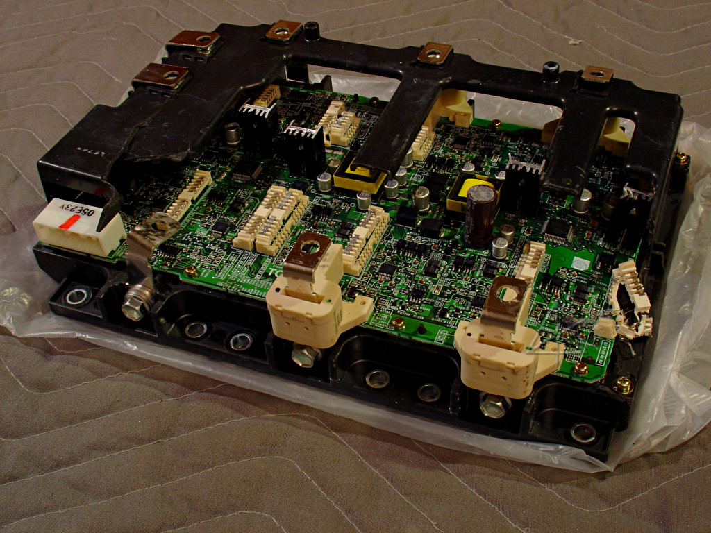
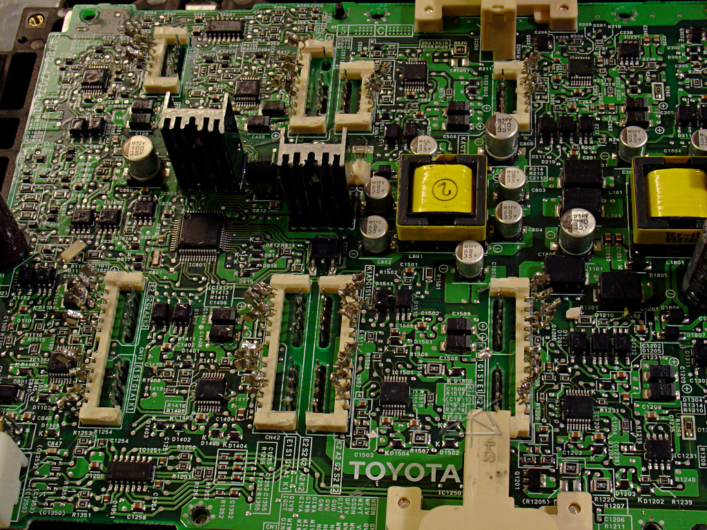
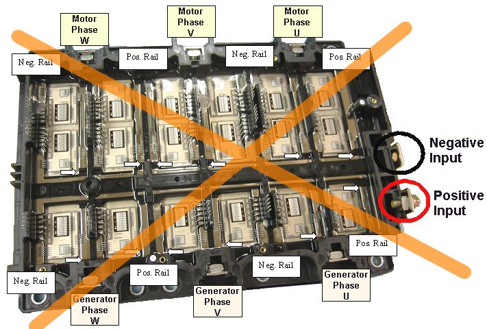
This is the main Integrated Power Module, or IPM, that drives the motors.
Control electronics on the visible board drive large IGBTs underneath.
The boosted positive and battery negative connect to the power rails of
the IGBT bridge pairs, and motor U/V/W emerge from the side terminals and
route upward toward where the MG1 and MG2 connections take off.  The large
off-white plastic assemblies around the connector straps are motor current
sensors.
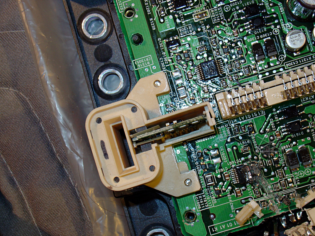
One of the current sensors with the little snap-on lid removed.  The V and W
leads have these; the current for the U connection can be deduced by the fact
that the motors have a simple Y connection and the three currents must sum
to zero.  These are full Hall-effect modules, not AC current transformers,
so they can indicate DC current levels in either direction.  It's also easy
to see how the board is conformal-coated over most of its surface [which also
makes part numbers that much harder to read].
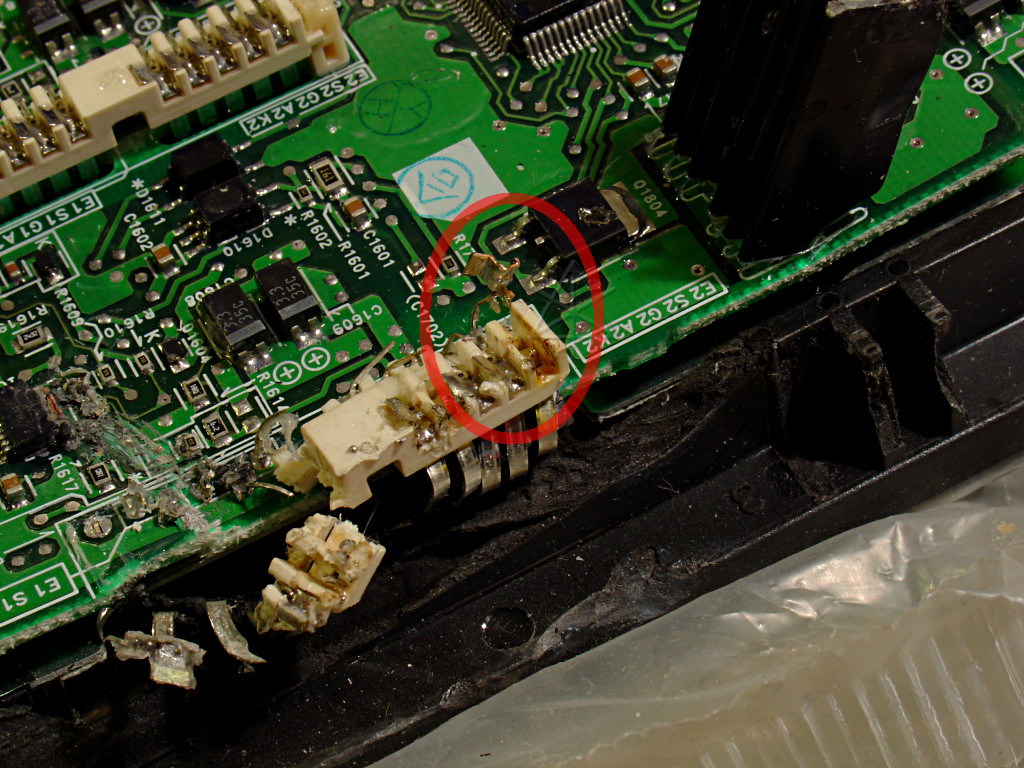
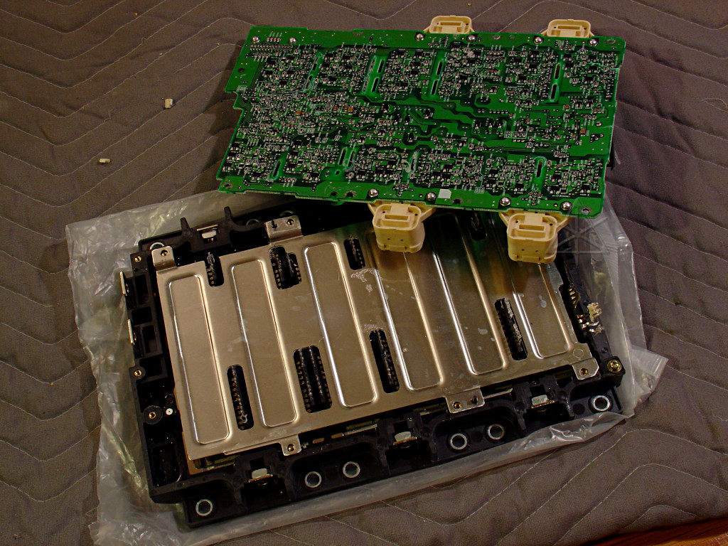
The "loose" IPM got fairly damaged in transit; the board is actually bent down
and cracked in this area.  With a multilayer board like this, it's probably
way past ever fixing.  Fortunately the one in the inverter is still intact.
Here we can see one of the many white connector blocks that go down to the
gate and other leads of the power transistors.  These aren't connectors that
can be unplugged; they all appear to simply be terminal points where soldered
connections are made.  One [circled] has been lifted so far, revealing no
simple way to disconnect these in bulk.
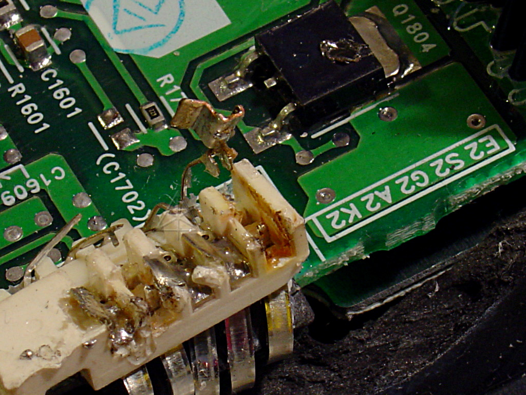
Which implies that if the board is going to come off the power-transistor
plate, every one of these has to be desoldered.  This is a multi-step
process -- they were likely originally done in parallel, after the board
was seated down and all the transistor leads simply poked up through the
holes in each of these lugs.  Now, since this board is relegated to demo
status, it's easier to heat each one and pull it up until the two little
retainer barbs come completely out of the plastic, allowing the lug to
bend back clear of the pin.
Some time later, all the lugs are finally desoldered and the retaining plastic
broken clear from around the pins, and the board is free to lift off ...
... revealing a shielding plate underneath.
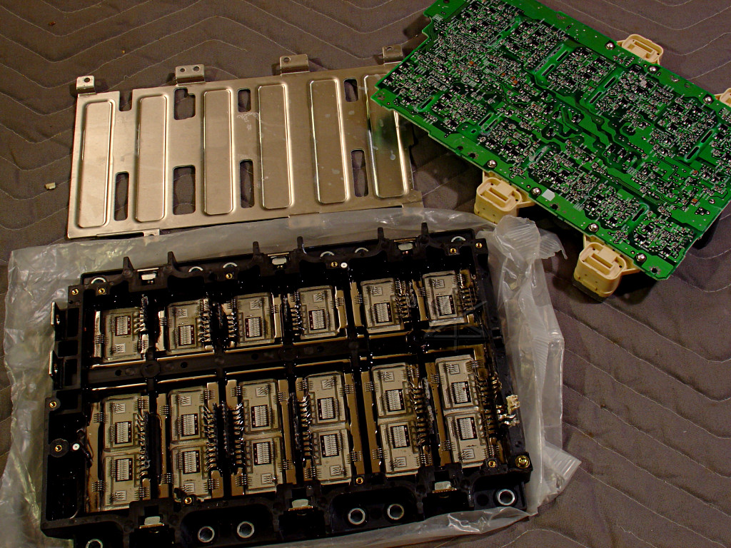
And after *that* is lifted off, we see the power transistor array.  This is
a view of electronics we usually only see when looking at highly magnified
pictures of transistor and integrated circuit dies -- slabs of silicon and
tiny bonding wires spot-welded in place.  This is the same type of construction
except it's on a scale easily viewable with the naked eye -- these things
are HUGE, and have multiple parallel bonding wires for high current capacity.
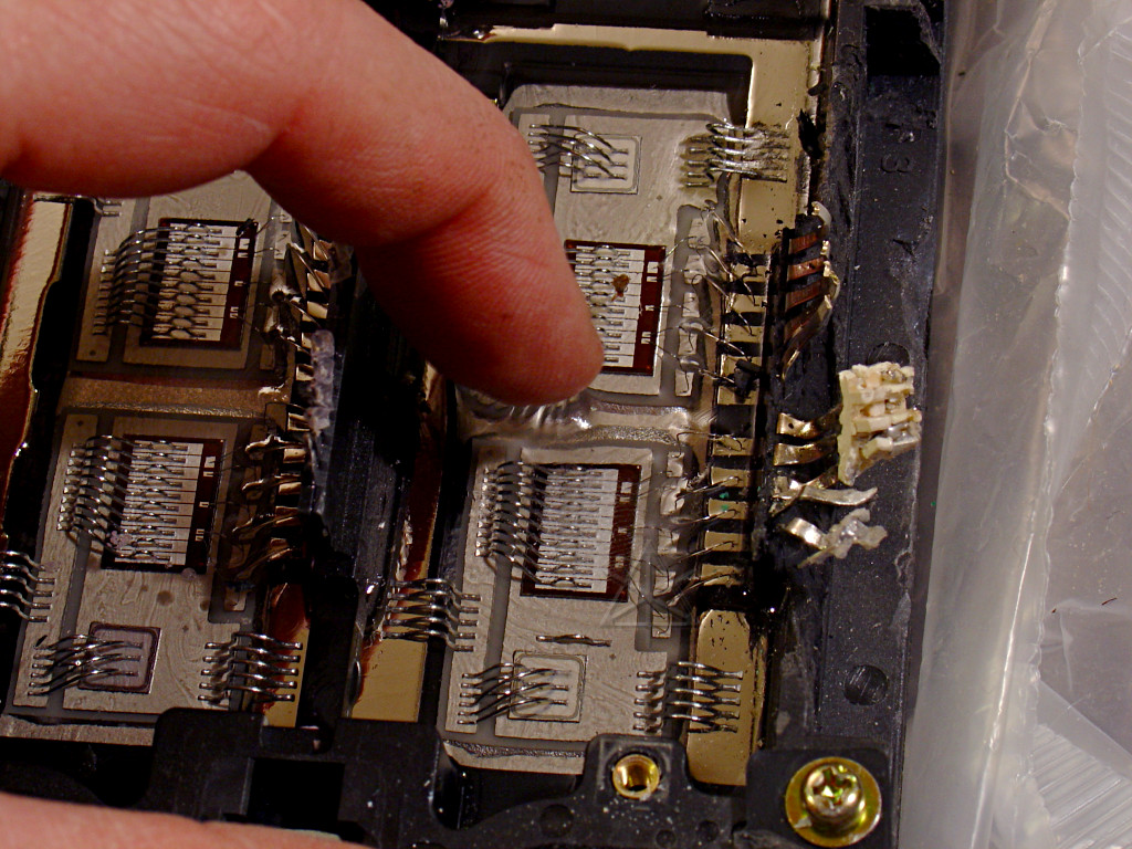
But the weirdest part is the layer of clear silicone potting goop that they're
all buried under.  This stuff really has to just be *experienced* to be
believed.  It's quite sticky but returns right down to its original layer when
poked and released, and is absolutely clear and very flat on the surface which
is why it's so easy to photograph through it.  It doesn't migrate or flow at
all; if it did, the mounting angle of the inverter would have caused it to all
pile up at one edge.  Oak Ridge possibly first brought all this to light and
has some pictures in 890029.pdf, but seeing and feeling the real thing here
really drives home how it's constructed.
The IGBTs for MG2 are doubled up for even higher current handling, and simply
connect in parallel.  This is Oakridge's determination of the overall power
routing -- except that they got it WRONG, reversing the positive and negative.
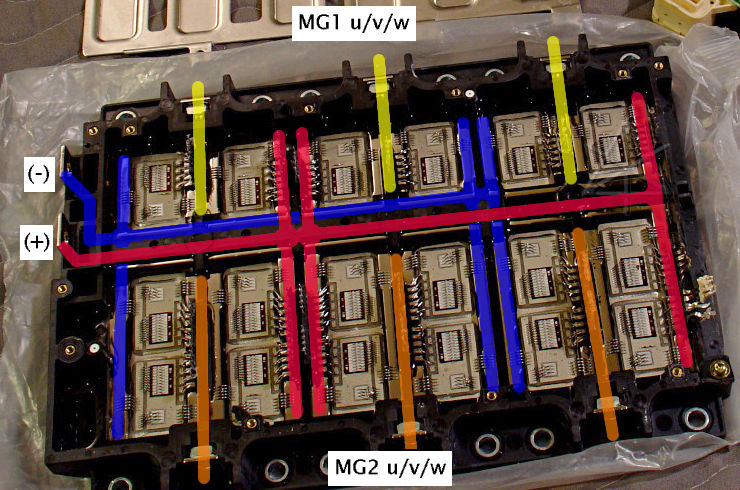
Here's how things are really connected inside the module.  The control
connections are always at the *collector* end of the transistor block; all
the V-phase devices in the center are flipped upside down to make the rail
routing simpler.  The rails are all embedded down in the plastic and the
routing is not obvious simply by looking at them.
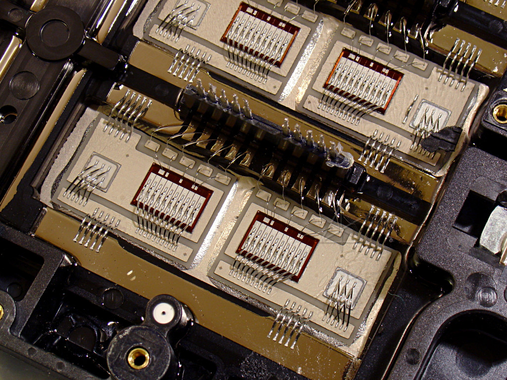
One of the transistor/diode pairs up close and personal.  The wires to the
control leads are surprisingly light and delicate -- they don't have to handle
a lot of current, but you'd think a little more physical robustness would be
desired in something that will later have potting compound poured into it.
The power bonding points, on the other hand, are heavy, numerous and spread
out to make current density through the devices as uniform as possible.

Sprinkled randomly around the whole IGBT array are little bonding-wire straps
bridging various points in the collector areas -- there's one visible in the
big version of this picture and several more in the ORNL shot above.  Their
locations are unstructured enough that my best guess would be post-construction
workarounds for layer nonuniformity, when test currents created hot spots and
revealed possible die defects.  Heat and thermal runaway will obviously be this
thing's worst enemy -- well-proven by some of the early device failures during
Prius development, which is why so much attention is paid to removing it and
why Toyota had to give up on off-the-shelf parts and develop their own IGBTs
for the purpose.
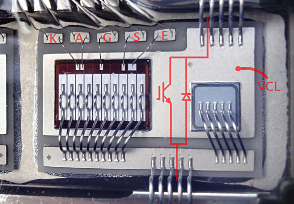
In fact, the design has evolved over time.  In particular, compare the diode
in this one, from ORNL's early '04 car, versus the previous from this '05
inverter -- a minor design change clearly happened in the interim, adding one
more bonding wire and changing the pattern across the anode pad.

Here, by the way, the leads have been labeled and the [correct!] equivalent
circuit overlaid.  There was a discussion on the Prius_Technical_Stuff
yahoogroup about some of this, and "toyolla2" offered the best explanation
for the five control leads:

	I believe we may be looking at the world's largest SENSFET !

	Motorola's tradename for the device which is able to indicate the
	current that's flowing in it. They are used for motor control when
	current sensing resistors become impractical due to dissipation and
	Ldi/dt issues.  An extra mosfet transistor is formed on the same die
	as the main device, thus it models the exact same current as the main
	device except that it has an die area 1/10000 the size and takes that
	fraction of main current.  A resistor of 200 ohms is connected from
	the source terminal S of this transistor which is brought out.  Also
	brought out is the Kelvin terminal, which I think is terminal E and
	goes to the emitters of the bipolar output transistor right on the
	die so that lead resistance and the accompanying offset voltage are
	avoided.  These two terminals usually feed into a differential
	amplifier.  The MC34129 current mode PWM chip interfaces quite well
	to these devices so you might find a tech bulletin on this chip to
	explain it more fully.

	Sensfets have five legs, this has seven. I think K and A are a diode
	being used as a die temperature sensing device.

In addition, the collector die from the MG1 U lead is brought out in a sixth
lead called "VCL", which one surmises simply monitors the common high-side
collector voltage which should closely equal the positive rail.  In general,
given the currents flowing through this assembly, it's clear that careful
attention has been given to detecting unusual voltage-drops through the
interconnects.
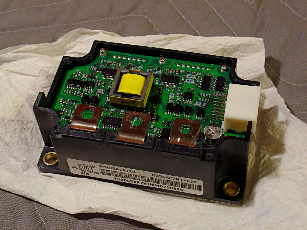
Next, we move on to the boost-converter module.  This drives the large
inductor next to it to raise the 220 or so battery volts up to as high as
500, to increase efficiency and available top speed of the motors.  The
faster a permanent-magnet motor spins, of course, the more voltage it
generates to fight the power supply which self-limits speed at a particular
voltage.  This is another IPM, similar in construction with a large heat-
sink plate underneath, heavy connections on the top, and a control-lead plug
in the side.

Trying to back out the screws holding the board down is, surprisingly, rather
futile.  They either spin without coming out, or are in so tight that I wound
up stripping the heads in the somewhat cheezy metal they're made of.  To try
and find out what was going on and if it's worth continuing, a small cut has
been made with a Dremel tool down past the board edge, and shining a light
through everything shows rather interestingly serpentine interconnect wires.
Again, hard-soldered in and no convenient connectors, implying another arduous
disconnection job.
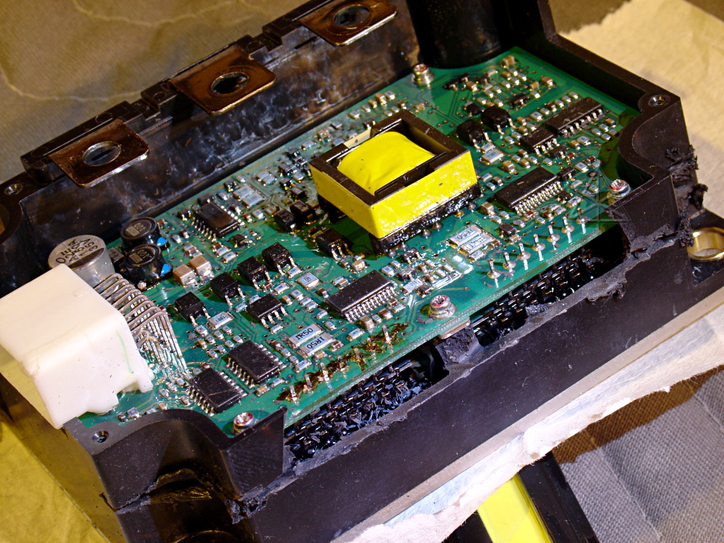
Finally, the entire front of the box is cut away, but despite that, still no
hints as to why the screws are, well, so screwed up.  Efforts [with somewhat
primitive tools at hand, the solder-sucker I *know* I have cannot be found
anywhere, argh] to desolder nicely aren't working well, so in disgust all the
interconnects simply get sliced and bunch of other nasty brute-force stuff
you really don't want to hear about happens in here.
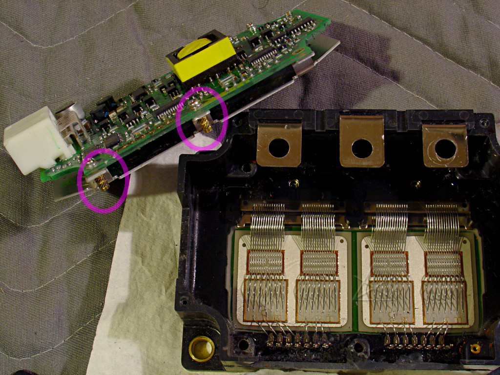
*Now* we see why the screws wouldn't come out.  Those stupid brass thread
inserts were poorly installed, and wound up just spinning in their holes.
Anyway, with the thing opened up at last we see very similar construction --
a thin shield layer under the driver board, and more power transistors
submerged in silicone goop.  ORNL also provided this detail, and hopefully
had better luck getting the thing apart.
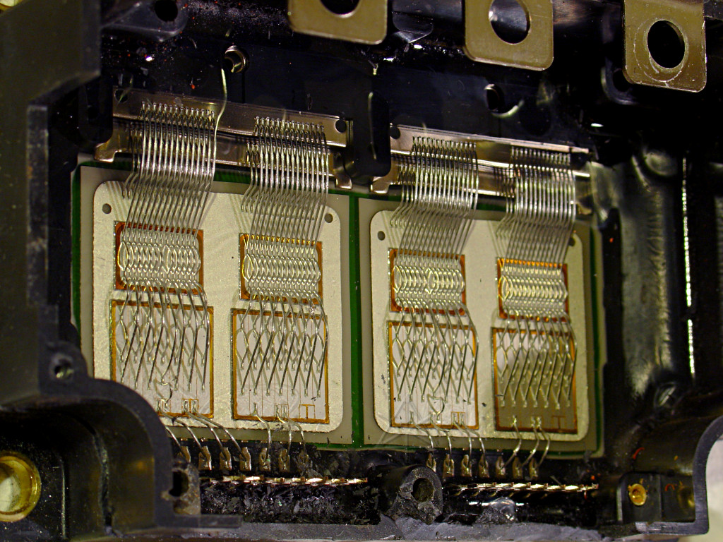
These transistors are even bigger!  Schematically this module has two power
IGBTs, but they're again doubled up with parallel pairs.  Where currents tend
to divide up through motor leads in the inverter IPM, this module has to
occasionally handle the full 100 amps available from or to the battery and
possibly much higher peak currents while doing boost switching, and it shows.
Even more attention is paid to bonding layout and sheer number of wires.  It's
interesting that the members of each pair are connected slightly differently,
with an additional tap extended right from the emitter to one of the sense
pads on one, and a separate connection on the other.  There's probably a good
reason behind that too, making every effort to sense conditions right down
at the device level.
_H* 070530