[Each picture is linked to a larger copy.]
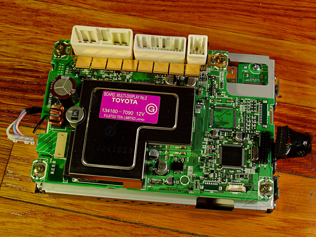
For completeness, I decided to take my own still-functional unit apart to see
if I could spot any differences in manufacturing that may have addressed the
connector-flakiness problem to make the later cars' displays more reliable.
The only difference visible here is that my unit has a "G" in a circle on
the pink label.  Underneath, some long part number in the white paint also
contains a "G" where the other MFD has "F".  That would imply a revision
difference.
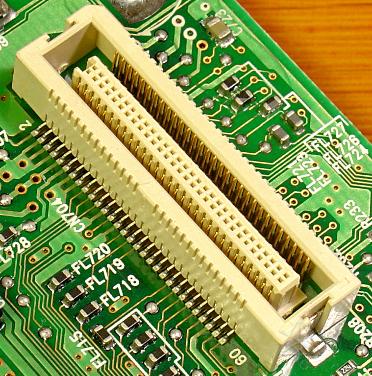
Looks like the same connector is used.  There aren't any visible maker or
part numbers on the connector so I don't even know who makes this one --
it may be underneath, entombed forever against the board.

Here we can sort of see the inverted "U" shaped lead-in pieces that can flex
to allow the center part of the shell to float around a little.  The outer
ends of those emerge as the surface-mount terminals down below.
Through the microscope, the soldering looks a little cleaner and more uniform,
but there is also less of the conformal coating splashed in against the
connector so it may just look better cosmetically.  But the surface-tension
fillets seem a little tighter than on the failed unit, which may indicate
slightly changed solder reflow parameters.
One thing to keep in mind that between 2004 and 2008 or so, we're in the
middle of the big RoHS changeover nightmare.  New types of lead-free solder
need slightly higher temperatures to flow, and component plastics and circuit
board materials must be sufficiently heat-resistant to survive the automated
soldering process.  The industry has experienced a lot of pain while re-
engineering its assembly lines, producing a few short-lived products that die
due to cold or cracked joints, tin whisker growth, hidden component damage,
moist-air surface corrosion, and who knows what else -- all because of the
concerns about lead and some other materials reaching the environment in
discarded electronics.  [Well, maybe if consumers weren't told repeatedly
that they need ANOTHER new computer or huge TV this year, this wouldn't be
quite such a problem.]

At this point, though, the electronics industry has mostly learned how to
adapt, and suppliers are providing some better-proven materials and being
able to specify how they will play together under certain heat ranges.
Better studies of the effects of thermal cycling under normal use have been
done as well.  While researching some of this as background for what might
be generically wrong with the MFD, I ran across some good references to round
out what I was vaguely groping for as potential reliability issues.

	http://www.globalsmt.net/content/view/967/118/  is entitled
	"Enhancing Pb-free Solder Joint Reliability", and discusses some
	of the techniques that can be used to mitigate stress issues in
	surface-mount parts and connections.

	http://www.apec-conf.org/2006/APEC_2006_SP4_5.pdf  is a set of
	slides about the effects of RoHS compliance changes on components
	and supplies.  Page 19 shows two amusing failure modes.  Parts have
	gotten so small that solder surface tension is a big issue, and if a
	board becomes too hot during assembly the layers can crack and
	separate. I'm really glad the MFD failure wasn't one of the latter --
	it would have been much more difficult to find, let alone fix.

Google for words like "rohs", "reflow", "wetting", "smt", etc for much more.

But could better process control be the whole answer to this?  I'm still not
convinced, and with both MFDs in front of me I can compare back and forth to
try and see if the soldering is really that different, or there's any other
visible characteristic that speaks to deliberate engineering improvements.
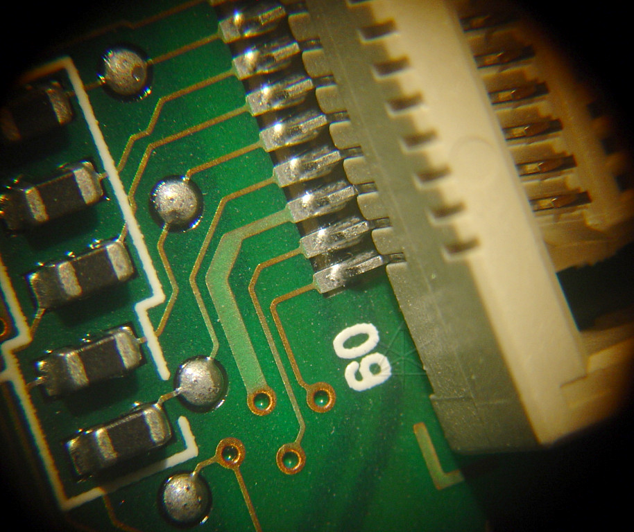
Here we're peeking way underneath that same connector on the good MFD, with an
LED flashlight shining a bluer light into the top and making a visible glint
off the back of the solder fillet.  A nice healthy connection, from the look
of it -- uniformly flowed all the way along, no cold patches, etc.  Use the
big pictures here to really see these details.
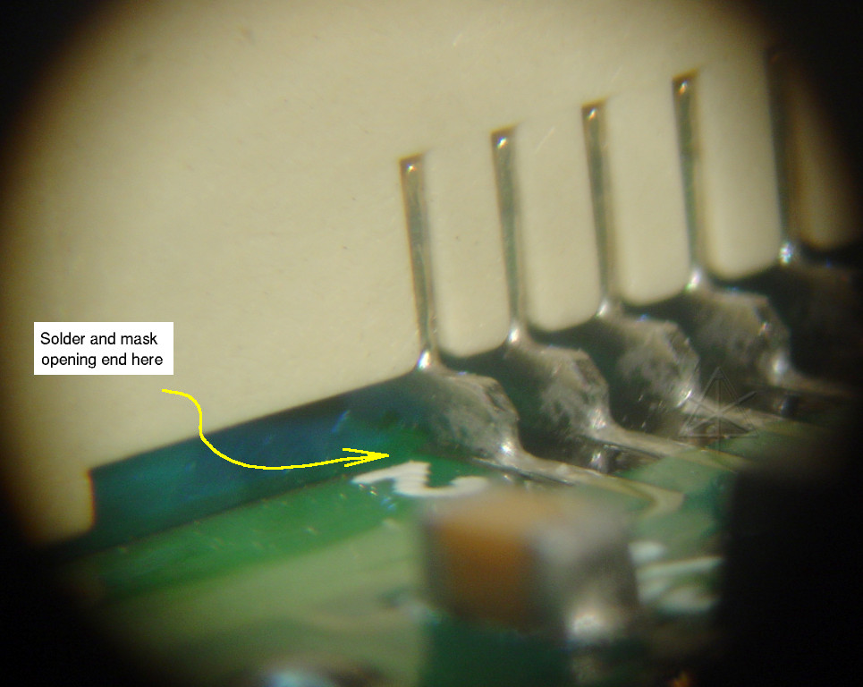
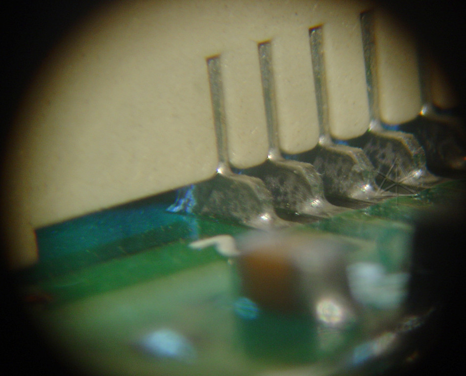
And finally, the same view under the bad one reveals the real change.  The pad
isn't long enough to extend under the entire foot of the connector lead, and
the solder flow was stopped by a smaller opening in the resist mask, so only
the outer part of the foot actually got tacked down.  It's got about a third
of the contact area that the good MFD has, in fact.  The connector lead is the
same, and is pretty clearly designed to be soldered all the way along with
a couple of midway cavities to help wick the metal underneath -- but in the
failed MFD, is severely starved for connection area.  The small blue glint at
the back of this one is from some of the conformal coating.

Here is an enlarged side-by-side view of the difference.

Interestingly, the terminals on the mating female half of the connector have
slightly different shapes which extend farther out and lend themselves to
longer pads, and have plenty of wetted contact area on both display boards.
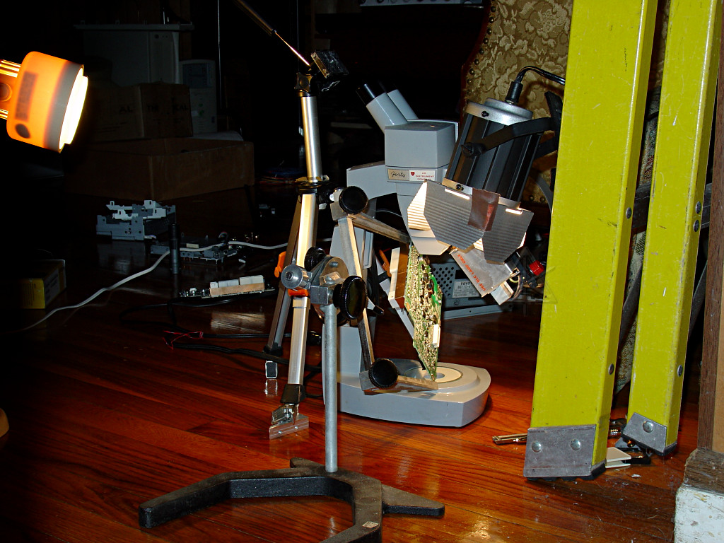
Getting these shots involved an amusingly complex setup, with a "third hand"
to hold the board, the tripod in *just* the right position for the camera to
see down the eyepiece of the scope, *lots* of lighting, and some dumb luck on
sizes of objects.  Here the camera is obviously not on the tripod.
It really looks like Fujitsu Ten screwed up on those early units, and failed
to design the circuit board lands to match the mounting spec for one half of
the connector chosen for the purpose.  The later change clearly shows that
someone either knew about or rediscovered the problem, and issued a quiet
ECO in the hope that the error wouldn't be noticed.  The owner community
certainly never heard anything about it, in contrast to, for example, the
steering-shaft recall.  I suppose not being able to control your cabin heat
on a cold night isn't considered a "life safety" issue?

In the meantime, Toyota is reaping the harvest from this error, a couple of
thousand dollars at a time, every time one of these defective units finally
yields to automotive-environment thermal and vibration stress and starts to
fail on an out-of-warranty owner.  A cost that high is even more ridiculous
considering that there's nothing in this unit any more sophisticated than a
modern computer motherboard, and what's that cost new, $200 or less?  While the
world is full of such injustices, here's one more that, when one is armed with
a little knowledge, accountability for can be shifted back toward the source,
or an enterprising DIYer can just work around.

The remaining question now is, how long is my two-pin rework likely to last?
If the crack began forming during uneven thermal stresses at manufacture, then
the fix could last forever since the reflow probably relieved stress -- or
since I might have mixed lead and non-lead solder, re-installation into a
car could shake-n-bake it loose in six months.  It could be an interesting
long-term observation.